PCB Production Guide: How Printed Circuit Boards Are Made
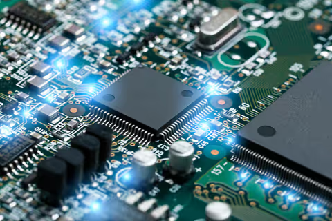
Printed Circuit Boards, commonly known as PCBs, form the foundation of modern electronic systems. They are flat boards that mechanically support and electrically connect electronic components using conductive pathways etched or printed onto insulating material. PCB production exists to organize complex electronic circuits into compact, reliable, and repeatable layouts.
Before PCB manufacturing processes were standardized, electronic circuits were built using point-to-point wiring. This approach was prone to errors, difficult to scale, and hard to maintain. PCB fabrication introduced a structured method that improved reliability, reduced size, and allowed consistent reproduction of electronic designs.
Today, PCB production plays a central role in devices such as smartphones, industrial controllers, medical equipment, networking hardware, and automotive electronics. As electronics continue to shrink and increase in complexity, PCB manufacturing techniques evolve to meet new design requirements.
Importance: Why PCB Production Matters Today
PCB production is essential because nearly every electronic product relies on it. From consumer electronics to critical infrastructure systems, PCBs ensure electrical stability, predictable performance, and efficient signal transmission.
This topic matters to multiple groups:
-
Electronics designers and engineers
-
Manufacturing and quality assurance teams
-
Technology students and researchers
-
Organizations working with hardware development
PCB manufacturing solves several technical challenges:
-
Organizing complex circuits in limited space
-
Reducing electrical noise and signal loss
-
Improving thermal management
-
Ensuring consistency across large production volumes
As industries adopt automation, artificial intelligence hardware, renewable energy systems, and connected devices, the demand for high-precision PCB fabrication continues to grow. Reliable PCB production directly affects product durability, safety, and long-term functionality.
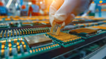
How Printed Circuit Boards Are Made: Core Production Stages
Design and Layout Preparation
PCB production begins with circuit design using electronic design automation software. Engineers create schematic diagrams and convert them into board layouts that define trace paths, component placement, and layer structure.
Key design elements include:
-
Trace width and spacing
-
Signal integrity planning
-
Power distribution paths
-
Ground planes
Design files are typically exported in standardized manufacturing formats to ensure compatibility with fabrication systems.
Material Selection and Lamination
Most PCBs use fiberglass-reinforced epoxy material with copper layers bonded on one or both sides. Multi-layer boards stack several conductive layers separated by insulating material.
The lamination process applies heat and pressure to bond layers into a single rigid structure. This stage determines board thickness, mechanical strength, and thermal stability.
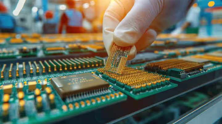
Imaging and Etching
The copper surface is coated with a light-sensitive material. A patterned image of the circuit layout is transferred onto the board using ultraviolet exposure.
Chemical etching removes unwanted copper, leaving behind conductive traces. Precision at this stage is critical to prevent short circuits or broken connections.
Drilling and Via Formation
Computer-controlled drilling machines create holes for component leads and vias. Vias allow electrical connections between different board layers.
There are several via types:
-
Through-hole vias
-
Blind vias
-
Buried vias
Accurate drilling ensures proper electrical connectivity and mechanical alignment.
Surface Finishing and Solder Mask Application
A solder mask is applied to protect copper traces from oxidation and prevent solder bridging during assembly. Surface finishes improve solderability and long-term reliability.
Common finishes include:
-
Hot air solder leveling
-
Electroless nickel immersion gold
-
Immersion silver
Each finish offers different performance characteristics depending on application requirements.
Recent Updates and Industry Trends in PCB Manufacturing
Over the past year, PCB production has continued to evolve in response to technological and environmental demands.
In 2025, manufacturers increasingly adopted advanced HDI (high-density interconnect) techniques to support compact device designs. Microvias and finer trace widths are becoming standard for high-performance electronics.
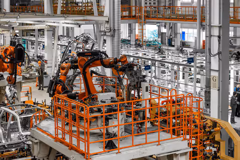
Automation and machine vision systems have expanded across fabrication lines, improving defect detection and process consistency. Artificial intelligence–assisted inspection tools gained broader adoption in late 2024 and early 2025.
Sustainability trends have also influenced PCB manufacturing. Many facilities introduced water recycling systems, lead-free processing methods, and energy-efficient lamination equipment to align with environmental compliance expectations.
Regulations and Policies Affecting PCB Production
PCB production is influenced by environmental and safety regulations in many countries. These rules aim to reduce hazardous substances and ensure responsible manufacturing practices.
Common regulatory considerations include:
-
Restrictions on lead and toxic materials
-
Wastewater treatment requirements
-
Air emission controls
-
Chemical handling and worker safety standards
In several regions, government initiatives support domestic electronics manufacturing by encouraging standardized quality certifications and environmentally compliant production methods.
Regulatory compliance plays a key role in maintaining product safety, international trade eligibility, and long-term sustainability of PCB fabrication operations.
Tools and Resources Used in PCB Production
A wide range of digital tools and technical resources support modern PCB manufacturing.
Design and planning tools often include:
-
PCB layout and schematic software
-
Signal integrity analysis tools
-
Thermal simulation platforms
Manufacturing support resources include:
-
Design rule checking utilities
-
Fabrication file validators
-
Stack-up planning templates
Reference documentation, material datasheets, and manufacturing standards provide guidance on best practices, tolerances, and quality benchmarks used throughout the PCB production lifecycle.
PCB Production Process Overview Table
| Production Stage | Purpose | Key Outcome |
|---|---|---|
| Circuit Design | Define electrical connections | Accurate layout files |
| Lamination | Bond material layers | Structural integrity |
| Etching | Remove excess copper | Precise conductive paths |
| Drilling | Create vias and holes | Layer connectivity |
| Finishing | Protect and prepare surfaces | Reliable soldering |
Common PCB Types and Applications
| PCB Type | Layer Count | Typical Use Case |
|---|---|---|
| Single-sided PCB | 1 | Basic electronics |
| Double-sided PCB | 2 | Power supplies |
| Multi-layer PCB | 4+ | Computing hardware |
| HDI PCB | High density | Compact devices |
Frequently Asked Questions About PCB Production
What materials are commonly used in PCB manufacturing?
Most PCBs use fiberglass epoxy laminate combined with copper layers. Specialized applications may use ceramic or flexible polymer materials.
How long does the PCB production process take?
Production timelines vary depending on board complexity, layer count, and testing requirements. Multi-layer boards typically require more processing stages.
Why are multiple layers used in PCBs?
Multi-layer designs allow more complex circuits in smaller spaces, improve signal control, and enhance power distribution.
What quality checks are performed during PCB fabrication?
Common inspections include electrical testing, optical inspection, and dimensional verification to detect defects or inconsistencies.
How does PCB production impact device reliability?
Accurate manufacturing ensures stable electrical connections, reduced signal interference, and long-term operational durability.
Conclusion: The Role of PCB Production in Modern Technology
PCB production remains a fundamental process in the electronics ecosystem. It transforms circuit designs into reliable physical structures that support modern digital systems. As devices become smaller, faster, and more interconnected, PCB manufacturing techniques continue to adapt through automation, precision engineering, and regulatory alignment.
Understanding how printed circuit boards are made provides insight into the unseen infrastructure that powers everyday technology. With ongoing advancements in materials, design tools, and manufacturing processes, PCB production will continue to support innovation across industries.